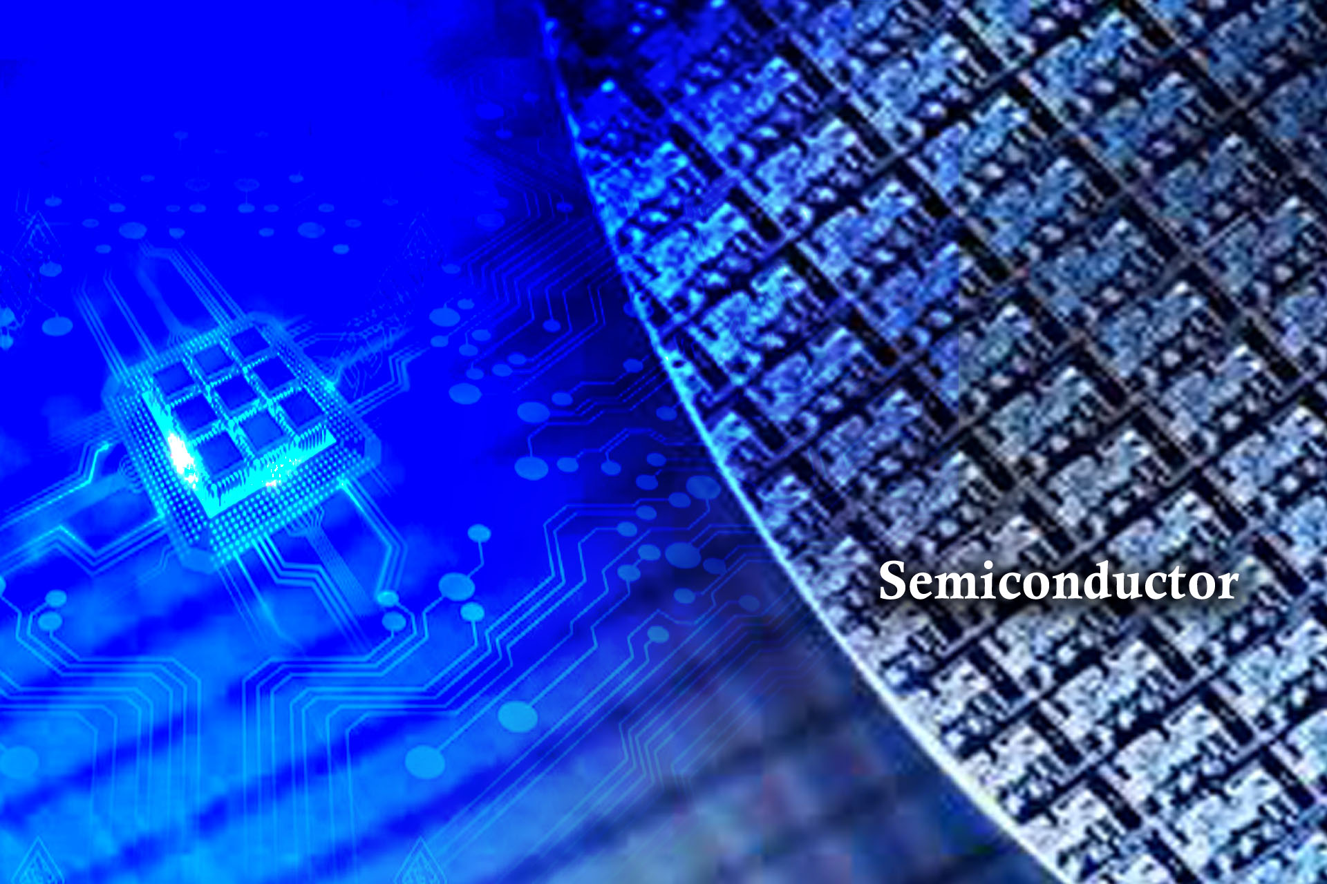
As the semiconductor market is moving towards using smaller and complex equipment and processes with smaller technology nodes ( 10nm and below ) , equipment with higher sensitivity is needed among manufacturers. Also, new materials and a more complex structure and design of such equipment must be developed.
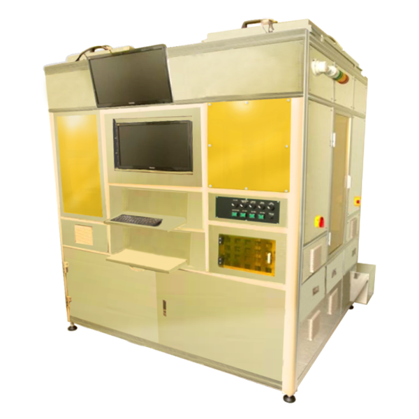
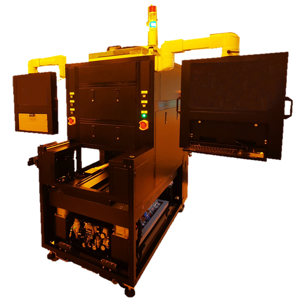
Mask inspection is to ensure the production quality of “Mask”, a tool used in semiconductor manufacturing. In wafer foundry, mask inspection equipment is used to detect defects on masks before preceding to Lithography. As the critical dimension of masks are becoming smaller, the complexity of process development and difficulty of mask inspection are as a result higher. Therefore, mask inspection equipment has to have higher precision in that the size, shape, and location of defects will be exposed onto the wafer, which will in turn affect the usage rate of the wafer. Nonetheless, keeping wafer production yield at a certain level requires close collaboration between foundries and mask shops.